
In context
In October 2025, the U.S. semiconductor industry was undergoing a strategic reshoring push, driven by the CHIPS Act and the need to secure advanced packaging capabilities for AI and high-performance computing. Amkor Technology's groundbreaking in Arizona marked a pivotal step in bringing high-volume advanced packaging to U.S. soil.
What was reported
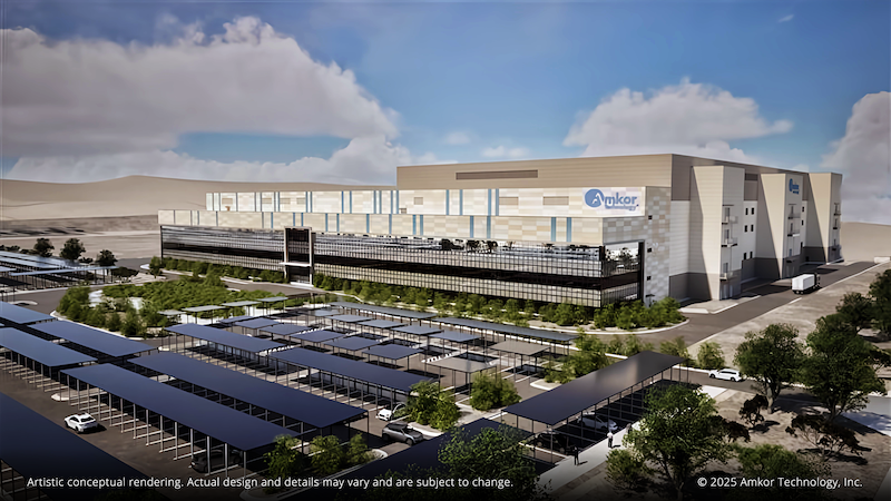
Amkor Technology announced an expanded investment of $7 billion for its new advanced packaging and test campus in Arizona, up by more than $5 billion from earlier plans. The expansion includes additional cleanroom space and a second greenfield facility, with construction of the first phase expected to complete by mid-2027 and production starting in early 2028.
Upon completion, the campus will offer over 750,000 square feet of cleanroom space and create up to 3,000 jobs. It will be the first U.S.-based high-volume advanced packaging facility, supporting key customers such as Apple and Nvidia. The project is backed by the CHIPS for America Program and the Advanced Manufacturing Investment Tax Credit.
The facility will feature smart factory technologies and scalable production lines for AI, high-performance computing, mobile, and automotive applications. It will complement TSMC's front-end wafer fabrication in Arizona, enabling end-to-end semiconductor manufacturing in the U.S.
Why it mattered
This investment signaled a major step toward onshoring the entire semiconductor supply chain, particularly advanced packaging, which is critical for AI chip performance. It underscored the growing trend of co-locating packaging with leading-edge fabrication to reduce supply chain risks and accelerate innovation in the U.S.
“This groundbreaking represents a bold step in Amkor’s long-term strategy for growth and innovation.”
Source: Robotics & Automation News (roboticsandautomationnews.com) · Published 2025-10-08 · “Amkor Technology to expand investment in Arizona campus to $7 billion”